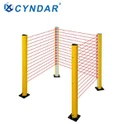
Solution: Laser scanner application in semiconductor wafer workshop
The area around the robotic arm in the semiconductor wafer workshop is very dangerous, and regional monitoring safety laser scanners are needed to monitor the surrounding environment.
When an object or person enters, the laser scanner will detect and control the robotic arm to stop working.
In the chip factory, the scanner detects the 0.2mm offset of the wafer box through 0.05° ultra-fine scanning. If the engineer enters the 0.5-meter clean area, the robotic arm enables nano-level suspension avoidance, and the non-contact path error is less than ±1μm, ensuring the safety of the production of hundreds of billions of chips.
Common design: The full solution supports NFC scene flash switching, adapts to different production line requirements in 5 minutes, passes mechanical safety certification, and realizes "detection-response-recovery" full closed-loop protection.

FAQ
1. How about your transportation?
A: Express delivery (sample order) or ocean shipping (bulk order) 2) Global transportation service is available 3) Please contact before ordering, because the transportation cost will change from time to time.
2. Does our lidar meet human eye safety standards? .
A: Our lidar meets human eye safety standards.
3. Can we visit your company?
A: Of course, you are always welcome. We can also pick you up at the airport and the station.